Difference between revisions of "L0I"
(→Interface) |
(→Detailed block diagram) |
||
| (13 intermediate revisions by the same user not shown) | |||
| Line 1: | Line 1: | ||
== Functionality Description == | == Functionality Description == | ||
| − | Level 0 Instruction Cache is accessed from the processor with only reads. It is a two | + | Level 0 Instruction Cache (L0i) is accessed from the processor with only reads. It is a two-stage blocking cache. A miss blocks all the newer requests. L0i always accepts the requests from processor or L1 cache (No busy by L0i). If there is a miss, incoming requests are buffered and replayed later by the cache. Therefore, the l0i replies to the processor requests in order. |
L0i does not send busy to the processor. The processor knows the L0i is busy if it doesn’t receive an ACK after | L0i does not send busy to the processor. The processor knows the L0i is busy if it doesn’t receive an ACK after | ||
sending two REQs. Then it stops sending REQs. On a miss, the L0I Cache sends a READLINE message to the L1 Cache. | sending two REQs. Then it stops sending REQs. On a miss, the L0I Cache sends a READLINE message to the L1 Cache. | ||
When the L1 cache has the requested data, it responds with a PUSHLINE message and the L0I Cache will fill the | When the L1 cache has the requested data, it responds with a PUSHLINE message and the L0I Cache will fill the | ||
| − | appropriate cache line with the received data. Every invalidation received from the L1 cache | + | appropriate cache line with the received data. Every invalidation received from the L1 cache invalidates |
| − | ALL the possible virtual cache lines. | + | ALL the possible virtual cache lines. |
| + | L0I -> L1 : READLINE | ||
| + | L1 -> L0I : PUSHLINE, INVALIDATE | ||
== Interface == | == Interface == | ||
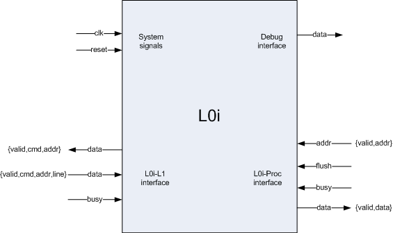
| − | L0i interface is divided into 4 | + | L0i interface is divided into 4 groups: processor interface, l1 interface, debug interface and system signals. |
Figure below shows the interface and the groups. '{}' shows that the associated signal is a structure composed of | Figure below shows the interface and the groups. '{}' shows that the associated signal is a structure composed of | ||
the members specified in it. | the members specified in it. | ||
| Line 19: | Line 21: | ||
[[Image:l0i-if.gif]] | [[Image:l0i-if.gif]] | ||
| − | == | + | == State Machines == |
| + | |||
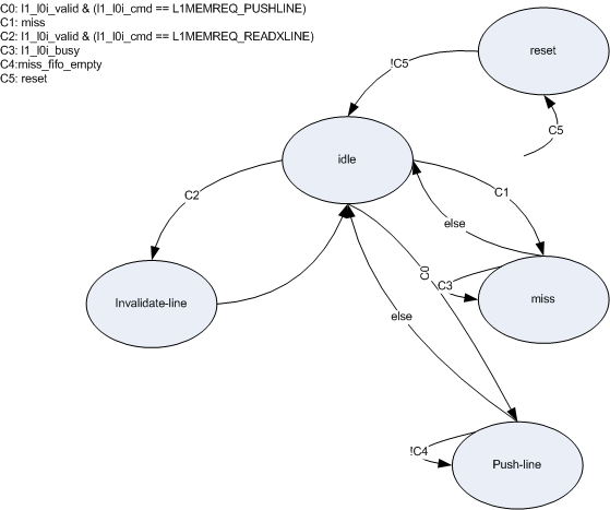
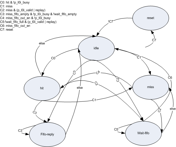
| + | Two state machines handle the communication to the outside, namely to processor and L1 cache. | ||
| + | |||
| + | L0i-L1 FSM: | ||
| + | |||
| + | [[Image:l0i-l1-fsm.gif]] | ||
| + | |||
| + | L0i-processor FSM: | ||
| + | |||
| + | [[Image:l0i-proc-fsm.gif]] | ||
| + | |||
| + | == Detailed block diagram == | ||
| + | |||
| + | |||
| + | [[Image:l0i-block-diagram.gif]] | ||
| + | |||
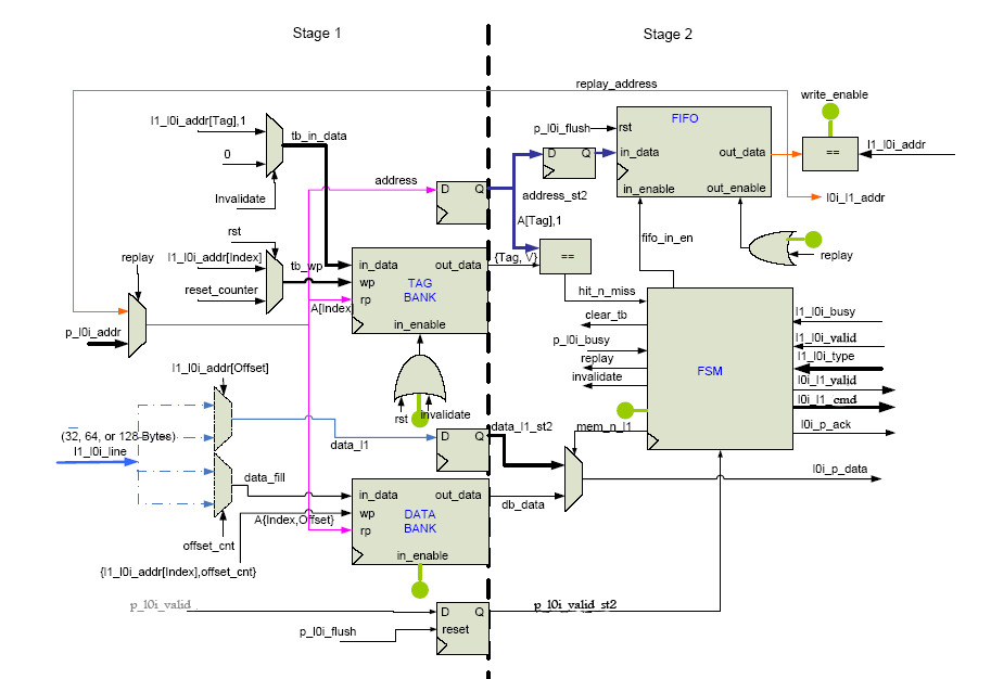
| + | This diagram may not match the last design. | ||
Latest revision as of 02:49, 1 June 2009
Functionality Description
Level 0 Instruction Cache (L0i) is accessed from the processor with only reads. It is a two-stage blocking cache. A miss blocks all the newer requests. L0i always accepts the requests from processor or L1 cache (No busy by L0i). If there is a miss, incoming requests are buffered and replayed later by the cache. Therefore, the l0i replies to the processor requests in order.
L0i does not send busy to the processor. The processor knows the L0i is busy if it doesn’t receive an ACK after sending two REQs. Then it stops sending REQs. On a miss, the L0I Cache sends a READLINE message to the L1 Cache. When the L1 cache has the requested data, it responds with a PUSHLINE message and the L0I Cache will fill the appropriate cache line with the received data. Every invalidation received from the L1 cache invalidates ALL the possible virtual cache lines.
L0I -> L1 : READLINE
L1 -> L0I : PUSHLINE, INVALIDATE
Interface
L0i interface is divided into 4 groups: processor interface, l1 interface, debug interface and system signals. Figure below shows the interface and the groups. '{}' shows that the associated signal is a structure composed of the members specified in it.
State Machines
Two state machines handle the communication to the outside, namely to processor and L1 cache.
L0i-L1 FSM:
L0i-processor FSM:
Detailed block diagram
This diagram may not match the last design.


