Difference between revisions of "SRAM 10T"
Tom Golubev (Talk | contribs) (Created page with '===Tom Golubev's F09 CMPE222 Project=== alt text') |
Tom Golubev (Talk | contribs) |
||
| (One intermediate revision by the same user not shown) | |||
| Line 2: | Line 2: | ||
| + | <p class="P2">Tom Golubev</p><p class="P2">CMPE 222 F09</p><p class="P2">10/12/09</p><p class="P2"> </p><p class="P1">VLSI Project Proposal</p><p class="P1"> </p><p class="P3">Extend the SRAM compiler to support 2 Read ports. This entails creating a 2 read port cell, making the compiler tile it, then adding more address decoders and sense amps. A high metal layer may be necessary (M3) for the decoders of the 2<span class="T1">nd</span> port. This project is half layout, half python compiler scripting.</p><p class="P3"> </p><p class="P3"> </p><p class="P3">* Denotes perceived difficulty, from low * to high ***</p><p class="P3"> </p><p class="P3">Basic Plan: </p><ul><li><p class="P4" style="margin-left: 0cm;"><span class="Bullet_20_Symbols" style="display: block; float: left; min-width: 0cm;">•.</span>*Understand Python script / study 1R/1W cell<span class="odfLiEnd"> </span></p></li><li><p class="P4" style="margin-left: 0cm;"><span class="Bullet_20_Symbols" style="display: block; float: left; min-width: 0cm;">•.</span>**Create / Simulate 2R/1W standard cell<span class="odfLiEnd"> </span></p></li><li><p class="P4" style="margin-left: 0cm;"><span class="Bullet_20_Symbols" style="display: block; float: left; min-width: 0cm;">•.</span>*Add 2R/1W option into compiler<span class="odfLiEnd"> </span></p></li><li><p class="P4" style="margin-left: 0cm;"><span class="Bullet_20_Symbols" style="display: block; float: left; min-width: 0cm;">•.</span>*Make compiler tile the 2R/1W cell<span class="odfLiEnd"> </span></p></li><li><p class="P4" style="margin-left: 0cm;"><span class="Bullet_20_Symbols" style="display: block; float: left; min-width: 0cm;">•.</span>*Figure out where to put address decoders / sense amps<span class="odfLiEnd"> </span></p></li><li><p class="P4" style="margin-left: 0cm;"><span class="Bullet_20_Symbols" style="display: block; float: left; min-width: 0cm;">•.</span>***Decide which metal layer 2<span class="T1">nd</span> read port interconnects will be on, metal3?<span class="odfLiEnd"> </span></p></li><li><p class="P4" style="margin-left: 0cm;"><span class="Bullet_20_Symbols" style="display: block; float: left; min-width: 0cm;">•.</span>***Have compiler wire interconnects for 2<span class="T1">nd</span> port<span class="odfLiEnd"> </span></p></li><li><p class="P4" style="margin-left: 0cm;"><span class="Bullet_20_Symbols" style="display: block; float: left; min-width: 0cm;">•.</span>**Test / Debug / validate<span class="odfLiEnd"> </span></p></li></ul><p class="P3"><span style=""></span></p><p class="P3">Extended Plan:</p><ul><li><p class="P5" style="margin-left: 0cm;"><span class="Bullet_20_Symbols" style="display: block; float: left; min-width: 0cm;">•.</span>*Simulate with CACTI<span class="odfLiEnd"> </span></p></li><li><p class="P5" style="margin-left: 0cm;"><span class="Bullet_20_Symbols" style="display: block; float: left; min-width: 0cm;">•.</span>**Try reducing area / power<span class="odfLiEnd"> </span> | ||
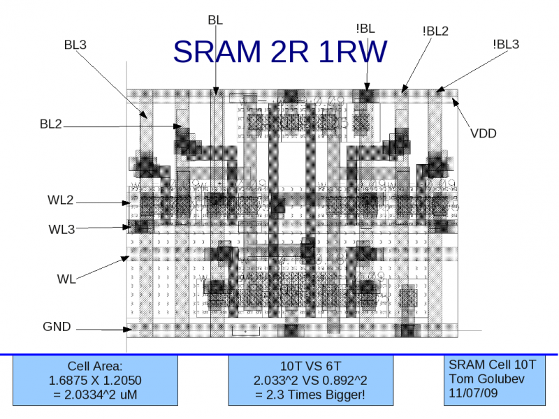
| − | + | [[File:10T_cell_present.png||800px|left|SRAM Cell Port Definitions]] | |
| − | [[File: | + | |
Latest revision as of 00:22, 8 November 2009
Tom Golubev's F09 CMPE222 Project
Tom Golubev
CMPE 222 F09
10/12/09
VLSI Project Proposal
Extend the SRAM compiler to support 2 Read ports. This entails creating a 2 read port cell, making the compiler tile it, then adding more address decoders and sense amps. A high metal layer may be necessary (M3) for the decoders of the 2nd port. This project is half layout, half python compiler scripting.
* Denotes perceived difficulty, from low * to high ***
Basic Plan:
•.*Understand Python script / study 1R/1W cell
•.**Create / Simulate 2R/1W standard cell
•.*Add 2R/1W option into compiler
•.*Make compiler tile the 2R/1W cell
•.*Figure out where to put address decoders / sense amps
•.***Decide which metal layer 2nd read port interconnects will be on, metal3?
•.***Have compiler wire interconnects for 2nd port
•.**Test / Debug / validate
Extended Plan:
•.*Simulate with CACTI
•.**Try reducing area / power
