Difference between revisions of "Running LVS"
(→LVS Options) |
|||
| (25 intermediate revisions by 4 users not shown) | |||
| Line 1: | Line 1: | ||
To run LVS, you must have a schematic and a DRC clean layout. | To run LVS, you must have a schematic and a DRC clean layout. | ||
| − | == | + | == LVS Options == |
| − | + | Similar to DRC, LVS in SCMOS is much easier than FreePDK45, because it uses Diva instead of Calibre. Select Verify -> Extract and then Verify->LVS and then fill in your schematic and extracted views. The LVS rules should be in the technology library already. | |
| − | + | For FreePDK45, if not done so already, Calibre->Setup->Layout Export. In the new window add the following path to the field '''User SKILL file''': | |
| − | + | /projects/cmpe122/techfiles/FreePDK45/ncsu_basekit/techfile/FreePDK45.tf | |
| − | == LVS | + | Then press OK and select Calibre->Run LVS. Like the DRC setup, select the LVS rules file: |
| + | |||
| + | /projects/cmpe122/techfiles/FreePDK45/ncsu_basekit/techfile/calibre/calibreLVS.rul | ||
| + | |||
| + | In the Input section, make sure you are comparing layout and netlist. It should be hierarchical. | ||
| + | |||
| + | Under the "Layout" tab, make sure the correct layout is selected and "Export from layout viewer" is selected. Under the "Netlist" tab make sure the correct top cell is selected and select "Export from schematic viewer". | ||
| + | [[Image:1-layout.jpg|center|400px]] | ||
| + | |||
| + | |||
| + | To turn on the advanced options, select Setup->LVS Options. This will add another option on the left called "LVS Options." Click it. In LVS Options, under the Supply tab, select "Ignore Layout and Source Pins during comparison". For some reason, our layout extractor is not extracting pin names at all. It will, however, make sure all the nets and transistors match correctly. | ||
| + | |||
| + | [[Image:3-options.jpg|center|400px]] | ||
| + | |||
| + | == Running LVS == | ||
| − | + | Click "Run LVS" to launch the job. It may warn you about overwriting files and such. That's ok. If things go well, you should match! You will see this: | |
| − | + | # ################### _ _ | |
| + | # # # * * | ||
| + | # # # CORRECT # | | ||
| + | # # # # \___/ | ||
| + | # ################### | ||
| − | |||
| − | |||
== Debugging errors == | == Debugging errors == | ||
There is a separate wiki page, [[Debugging LVS]], on suggestions for debugging errors. This is a very difficult problem sometimes, but it is usually a simple swap of nets or pins. | There is a separate wiki page, [[Debugging LVS]], on suggestions for debugging errors. This is a very difficult problem sometimes, but it is usually a simple swap of nets or pins. | ||
Latest revision as of 18:27, 21 March 2014
To run LVS, you must have a schematic and a DRC clean layout.
LVS Options
Similar to DRC, LVS in SCMOS is much easier than FreePDK45, because it uses Diva instead of Calibre. Select Verify -> Extract and then Verify->LVS and then fill in your schematic and extracted views. The LVS rules should be in the technology library already.
For FreePDK45, if not done so already, Calibre->Setup->Layout Export. In the new window add the following path to the field User SKILL file:
/projects/cmpe122/techfiles/FreePDK45/ncsu_basekit/techfile/FreePDK45.tf
Then press OK and select Calibre->Run LVS. Like the DRC setup, select the LVS rules file:
/projects/cmpe122/techfiles/FreePDK45/ncsu_basekit/techfile/calibre/calibreLVS.rul
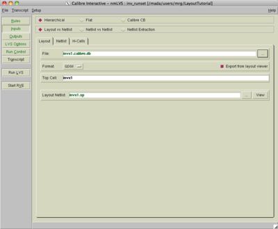
In the Input section, make sure you are comparing layout and netlist. It should be hierarchical.
Under the "Layout" tab, make sure the correct layout is selected and "Export from layout viewer" is selected. Under the "Netlist" tab make sure the correct top cell is selected and select "Export from schematic viewer".
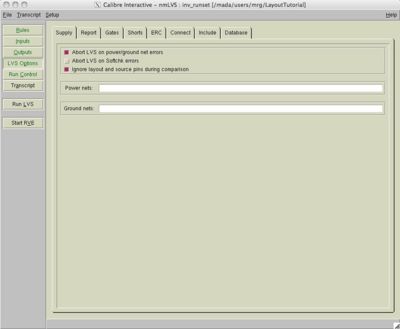
To turn on the advanced options, select Setup->LVS Options. This will add another option on the left called "LVS Options." Click it. In LVS Options, under the Supply tab, select "Ignore Layout and Source Pins during comparison". For some reason, our layout extractor is not extracting pin names at all. It will, however, make sure all the nets and transistors match correctly.
Running LVS
Click "Run LVS" to launch the job. It may warn you about overwriting files and such. That's ok. If things go well, you should match! You will see this:
                        #       ###################       _   _
                       #        #                 #       *   *
                  #   #         #     CORRECT     #         |
                   # #          #                 #       \___/
                    #           ###################
Debugging errors
There is a separate wiki page, Debugging LVS, on suggestions for debugging errors. This is a very difficult problem sometimes, but it is usually a simple swap of nets or pins.

