Difference between revisions of "Implementing State Machines using Verilog for the logic"
| (One intermediate revision by one other user not shown) | |||
| Line 3: | Line 3: | ||
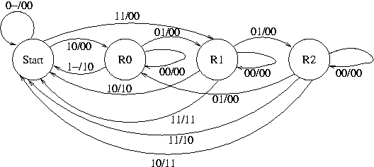
To illustrate the process we will use a sequential circuit with two synchronous inputs x and y, and two outputs z and w. In this example the input x is a marker indicating the start and stop of a sequence of data bits which appear on input y. When x is high at the clock edge, the sequence starts with the current value on y and continues until the next clock edge where x is high. The output z should be high on the clock edge where the sequence stops: effectively, every other edge where x is high. The output w should be high at the same time as z but only if the number of 1's on the clock edges between the start and stop is 2 (modulo 3). | To illustrate the process we will use a sequential circuit with two synchronous inputs x and y, and two outputs z and w. In this example the input x is a marker indicating the start and stop of a sequence of data bits which appear on input y. When x is high at the clock edge, the sequence starts with the current value on y and continues until the next clock edge where x is high. The output z should be high on the clock edge where the sequence stops: effectively, every other edge where x is high. The output w should be high at the same time as z but only if the number of 1's on the clock edges between the start and stop is 2 (modulo 3). | ||
| − | [[File:fsm_ex. | + | [[File:fsm_ex.gif]] |
With the minimum length state encoding (Q1, Q0) below | With the minimum length state encoding (Q1, Q0) below | ||
| Line 69: | Line 69: | ||
[[File:fsm1_sch.jpg]] | [[File:fsm1_sch.jpg]] | ||
| + | |||
| + | |||
| + | The CMPE100 Web: | ||
| + | Copyright 2011; Department of Computer Engineering, University of California, Santa Cruz. | ||
Latest revision as of 23:39, 23 March 2011
This page decribes how to implement a state machine using a combination of schematics and Verilog for the next state and output logic.
To illustrate the process we will use a sequential circuit with two synchronous inputs x and y, and two outputs z and w. In this example the input x is a marker indicating the start and stop of a sequence of data bits which appear on input y. When x is high at the clock edge, the sequence starts with the current value on y and continues until the next clock edge where x is high. The output z should be high on the clock edge where the sequence stops: effectively, every other edge where x is high. The output w should be high at the same time as z but only if the number of 1's on the clock edges between the start and stop is 2 (modulo 3).
With the minimum length state encoding (Q1, Q0) below
State 	Q1 Q0
Start 	0 0
R0 	0 1
R1 	1 0
R2 	1 1
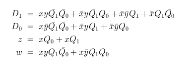
we came up with the following equations for the next state and outputs:
The Verilog code for this logic is:
module fsm_logic(x,y,Q,z,w,D);
  input x;
  input y;
  input [1:0] Q;
  output z;
  output w;
  output [1:0] D;
  assign D[1] = x&y&~Q[1]&~Q[0] | ~x&y&Q[0]&~Q[1] | ~x&~y&Q[1] | ~x&~Q[0]&Q[1];
  assign D[0] = x&~y&~Q[1]&~Q[0] | ~x&y&Q[1] | ~x&~y&Q[0];
  assign z = x&Q[0] | x&Q[1];
  assign w = x&y&Q[1]&~Q[0] | x&~y&Q[1]&Q[0];
endmodule
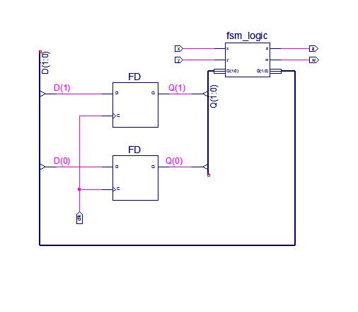
The state machine is implemented in the schematic below by adding two flip-flops (FD) and including the symbol for the state machine logic. Since the encoding for our start state was Q1Q0=00, the global reset will put our machine into the Start state.
If instead we use one-hot encoding:
State 	Q3  Q2  Q1  Q0
Start 	0   0   0   1
R0 	0   0   1   0
R1 	0   1   0   0
R2 	1   0   0   0
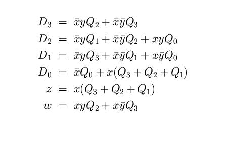
we would obtain the following equations for the next state and outputs:
The Verilog code for this logic is:
module fsm_logic(x,y,Q,z,w,D);
   input x;
   input y;
   input [3:0] Q;
   output z;
   output w;
   output [3:0] D;
   assign D[3] = ~x&y&Q[2] | ~x&~y&Q[3];
   assign D[2] = ~x&y&Q[1] | ~x&~y&Q[2] | x&y&Q[0];
   assign D[1] = ~x&y&Q[3] | ~x&~y&Q[1] | x&~y&Q[0];
   assign D[0] = ~x&Q[0] | x&(Q[3]|Q[2]|Q[1]);
   assign z = x & (Q[3]|Q[2]|Q[1]);
   assign w = x&y&Q[2] | x&~y&Q[3];
endmodule
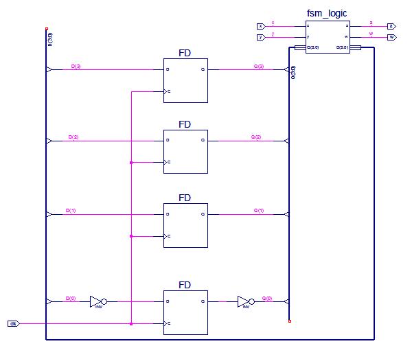
The state machine is implemented in the schematic below by adding 4 flip-flops (FD) and including the symbol for the state machine logic. We would like the global reset to put our machine into the Start state (Q3Q2Q1Q0=0001). To make this happen we put inverters around the flip-flop holding Q0. The only effect this has is to make Q0 = 1 on reset.
The CMPE100 Web:
Copyright 2011; Department of Computer Engineering, University of California, Santa Cruz.
