Difference between revisions of "Running DRC"
(→Running DRC) |
(→Running DRC) |
||
| (20 intermediate revisions by 4 users not shown) | |||
| Line 1: | Line 1: | ||
| + | <div style="float:left" align=left>[[INV_Layout_Tutorial |<--4. INV Layout Tutorial]]</div><div style="float:right" align=right>[[Running_LVS|6. Running LVS-->]]</div> | ||
| + | |||
| + | |||
== Running DRC == | == Running DRC == | ||
| − | + | For SCMOS, running DRC just requires you to select "Verify->DRC". | |
| − | + | For FreePDK45, however, it uses Calibre. | |
| − | + | Select Calibre->Run DRC from the top menus. This will open two new windows for DRC as shown here: | |
| − | + | ||
| + | [[Image:1-load_runset.jpg|center|300px]] | ||
| + | [[Image:2-calibre_interactive.jpg|center|300px]] | ||
| + | |||
| + | Press "Cancel" on the runset window -- we won't use this. Click the "Rules" button on the interactive window and navigate to the Calibre rules file here: | ||
| + | |||
| + | /projects/cmpe122/techfiles/FreePDK45/ncsu_basekit/techfile/calibre/calibreDRC.rul | ||
| + | |||
| + | Click on the "Run DRC" button and you will get two more windows. The first one shows a summary of all the shapes and rules checked: | ||
| + | [[Image:3-drc_summary.jpg|center|300px]] | ||
== Viewing errors == | == Viewing errors == | ||
| − | + | The second window summarizes the errors: | |
| + | [[Image:4-error_summary.jpg|center|300px]] | ||
| − | |||
| − | |||
| − | |||
| − | |||
| − | |||
| − | It may be obvious once you see the error where the problem is, but sometimes you need to investigate a little bit. If you | + | It may be obvious once you see the error where the problem is, but sometimes you need to investigate a little bit. If you click on a rule and expand it, it will show the associated errors. If you click the error, it will be highlighted in your layout window. |
| + | |||
| + | Typically, these will show that two shapes are too close, too narrow, or something similar. The errors even refer to the SCMOS rule that is violated. If you don't understand, look it up on the [http://www.eda.ncsu.edu/wiki/FreePDK45:Contents#User_Guide FreePDK45 design rule guide]. Now, fix all of the errors so it is DRC clean! | ||
== Common errors == | == Common errors == | ||
A common problem with DRC is when you instantiate cells. If there is not enough space from a shape inside a cell to a shape inside another cell, you will get an error. In other words, DRC is done flat. If you remove all hierarchy, you must pass DRC. Think about this when you make your cells by leaving at least 1/2 of a spacing rule between a shape and the edges of a cell. The edges of a cell are the bounding box of all shapes. | A common problem with DRC is when you instantiate cells. If there is not enough space from a shape inside a cell to a shape inside another cell, you will get an error. In other words, DRC is done flat. If you remove all hierarchy, you must pass DRC. Think about this when you make your cells by leaving at least 1/2 of a spacing rule between a shape and the edges of a cell. The edges of a cell are the bounding box of all shapes. | ||
| + | |||
| + | Another common problem is the contact overlap parameter in the PMOS/NMOS PCell. Make sure that diffContactLeftCov and diffContactRightCov are set to 0 otherwise you will get a poly-diffusion spacing error for small transistors. | ||
| + | |||
| + | Another common problem is with n- and p-wells. Often you will have many shapes abuting in complex ways. To avoid DRC issues, it is common to put a big rectangle of nwell or pwell over the whole area to simplify it. Overlapping shapes just results in a single opening in the mask that is a union of all shapes and is not a problem. | ||
| + | |||
| + | The pdcont and ndcont don't seem to make the active area big enough. In order to fix this, you need to expand the active to 90nm in all dimensions. | ||
| + | |||
| + | A correct layout (with the wrong sizes and heights for your homework!) and summary will look something like this: | ||
| + | |||
| + | [[Image:5-correct_rve.jpg|center|300px]] | ||
| + | [[Image:6-correct_layout.jpg|center|400px]] | ||
| + | |||
| + | |||
| + | <div style="float:left" align=left>[[INV_Layout_Tutorial |<--4. INV Layout Tutorial]]</div><div style="float:right" align=right>[[Running_LVS|6. Running LVS-->]]</div> | ||
Latest revision as of 18:23, 21 March 2014
Running DRC
For SCMOS, running DRC just requires you to select "Verify->DRC".
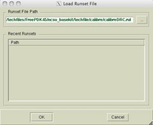
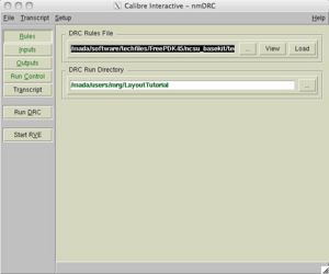
For FreePDK45, however, it uses Calibre. Select Calibre->Run DRC from the top menus. This will open two new windows for DRC as shown here:
Press "Cancel" on the runset window -- we won't use this. Click the "Rules" button on the interactive window and navigate to the Calibre rules file here:
/projects/cmpe122/techfiles/FreePDK45/ncsu_basekit/techfile/calibre/calibreDRC.rul
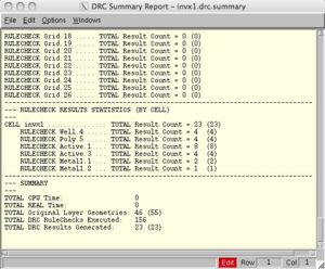
Click on the "Run DRC" button and you will get two more windows. The first one shows a summary of all the shapes and rules checked:
Viewing errors
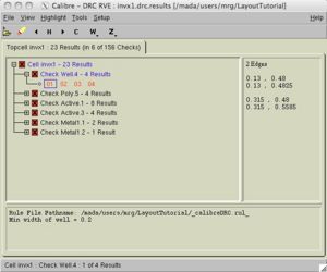
The second window summarizes the errors:
It may be obvious once you see the error where the problem is, but sometimes you need to investigate a little bit. If you click on a rule and expand it, it will show the associated errors. If you click the error, it will be highlighted in your layout window.
Typically, these will show that two shapes are too close, too narrow, or something similar. The errors even refer to the SCMOS rule that is violated. If you don't understand, look it up on the FreePDK45 design rule guide. Now, fix all of the errors so it is DRC clean!
Common errors
A common problem with DRC is when you instantiate cells. If there is not enough space from a shape inside a cell to a shape inside another cell, you will get an error. In other words, DRC is done flat. If you remove all hierarchy, you must pass DRC. Think about this when you make your cells by leaving at least 1/2 of a spacing rule between a shape and the edges of a cell. The edges of a cell are the bounding box of all shapes.
Another common problem is the contact overlap parameter in the PMOS/NMOS PCell. Make sure that diffContactLeftCov and diffContactRightCov are set to 0 otherwise you will get a poly-diffusion spacing error for small transistors.
Another common problem is with n- and p-wells. Often you will have many shapes abuting in complex ways. To avoid DRC issues, it is common to put a big rectangle of nwell or pwell over the whole area to simplify it. Overlapping shapes just results in a single opening in the mask that is a union of all shapes and is not a problem.
The pdcont and ndcont don't seem to make the active area big enough. In order to fix this, you need to expand the active to 90nm in all dimensions.
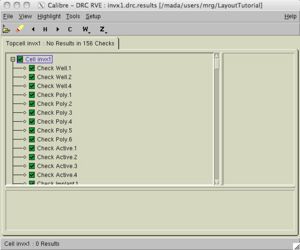
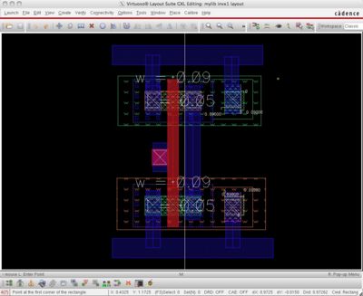
A correct layout (with the wrong sizes and heights for your homework!) and summary will look something like this:
