Difference between revisions of "Back Annotation"
(→Extract Parasitics) |
|||
| Line 18: | Line 18: | ||
* The .pxi file ("invx1.pex.netlist.INVX1.pxi") contains the connections between the parasitics and the transistors. | * The .pxi file ("invx1.pex.netlist.INVX1.pxi") contains the connections between the parasitics and the transistors. | ||
| − | |||
| − | + | If the above simulation gets too slow, you can run without resistive parasitics but with less accuracy. To do this, change the extraction type to "C+CC" instead of "R+C+CC". | |
| + | Now, you are ready to run a back-annotated simulation. | ||
| − | + | == Back-Annotated Simulation == | |
| + | |||
| + | [[Image:simulatebackannotated.jpg|400px]] | ||
Revision as of 21:12, 1 October 2009
The above simulation did not actually include the parasitic capacitances and resistances of the interconnect. Spectre (or hSpice) will by default use the gate area (L and W) to estimate the gate capacitance, but additional poly is not considered. If you specified perimeters (ps, pd) and areas (as, ad) in the pcell form, it will include those estimates in simulation. However, it does not include any extra routing, contacts, diffusion, etc. In order to include these, you need to perform parasitic extraction and back-annotation. The extraction is similar to the device extraction you used to extract a netlist for LVS, but now it extracts parasitic resistances and capacitances too.
Your design must pass DRC and LVS to do this.
Extract Parasitics
This is very similar to LVS. Go to Calibre->Run PEX. You will need to specify a layer map like LVS again. Also, select the rule file as this:
/mada/software/techfiles/FreePDK45/ncsu_basekit/techfile/calibrexRC.rul
Under the Input section, in the Layout tab, make sure that GDSII and "Export from layout viewer" are selected. Under the Netlist tab, make sure that SPICE and "Export from schematic viewer" are selected.
Under the Output section, most options should be left as default. By default, "All Nets" under the Nets tab should be checked. Under the Report tab, select "Generate PEX report" and "View report after PEX finishes". Under SVDB, make sure that "Start RVE after PEX" is checked.
After this, there are a few files that were created
- The .pex file ("invx1.pex.netlist.pex") contains all of the parasitics in a hierarchical format like spice.
- The actual netlist ("NAND2.pex.netlist") with only the transistors is the .netlist file.
- The .pxi file ("invx1.pex.netlist.INVX1.pxi") contains the connections between the parasitics and the transistors.
If the above simulation gets too slow, you can run without resistive parasitics but with less accuracy. To do this, change the extraction type to "C+CC" instead of "R+C+CC".
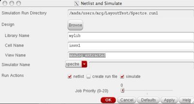
Now, you are ready to run a back-annotated simulation.
