Difference between revisions of "Entering a schematic"
| Line 9: | Line 9: | ||
2. Double click on the top level schematic (world.sch) in the top left pane of the Project Navigator. | 2. Double click on the top level schematic (world.sch) in the top left pane of the Project Navigator. | ||
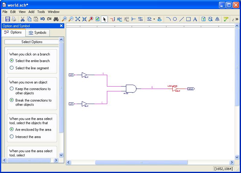
| − | 3. The schematic editor will display your (currently empty) schematic in the right pane. Click on the [[File: | + | 3. The schematic editor will display your (currently empty) schematic in the right pane. Click on the [[File:float_icon.jpg]] icon to pull it out and get the window below. |
[[File:schematic1.jpg]] | [[File:schematic1.jpg]] | ||
Revision as of 20:52, 21 March 2011
This is an EXAMPLE only. The schematic that you will need to enter for Lab 1 has additional gates and I/Os. These instructions will take you through the steps needed to enter a simple schematic. It is assumed that you have already created a project with an empty schematic. If not. follow the instructions for Creating a new project.
1. Open your project in the Project Navigator, either by double clicking on the file project_name.ise in
C:\Documents and Settings\your_login\Desktop\project_name.
This file should have a thumbnail that looks like the Project Navigator icon. You can also open your project by double clicking the Project Navigator icon on the Desktop and then selecting Open Project from the File menu and selecting the same file.
2. Double click on the top level schematic (world.sch) in the top left pane of the Project Navigator.
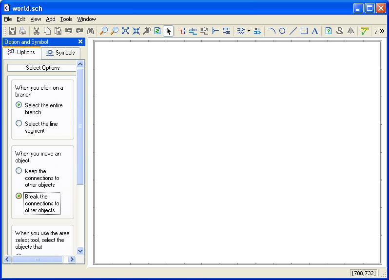
3. The schematic editor will display your (currently empty) schematic in the right pane. Click on the ![]() icon to pull it out and get the window below.
icon to pull it out and get the window below.
The left pane of the schematic editor window has two tabs: Symbols and Options. (If you ever need to reopen the left pane, under the View menu check the Options and Symbol box.)
The right pane is where your schematic will be drawn.
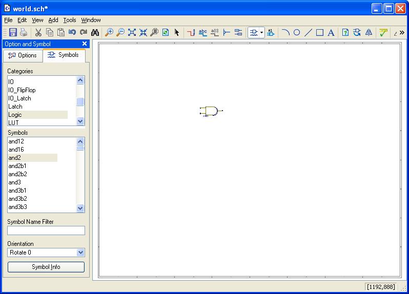
4. Click the Symbol tab. The symbols are divided into categories in the upper window.
Click on the ![]() icon and then select Logic and click on and2. Move the cursor to the drawing window and click when you have the and gate where you want to place it.
icon and then select Logic and click on and2. Move the cursor to the drawing window and click when you have the and gate where you want to place it.
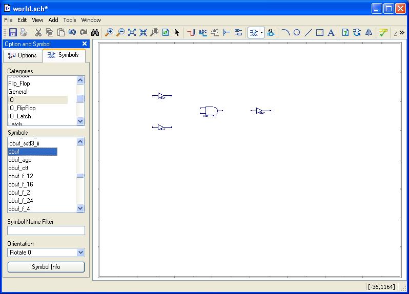
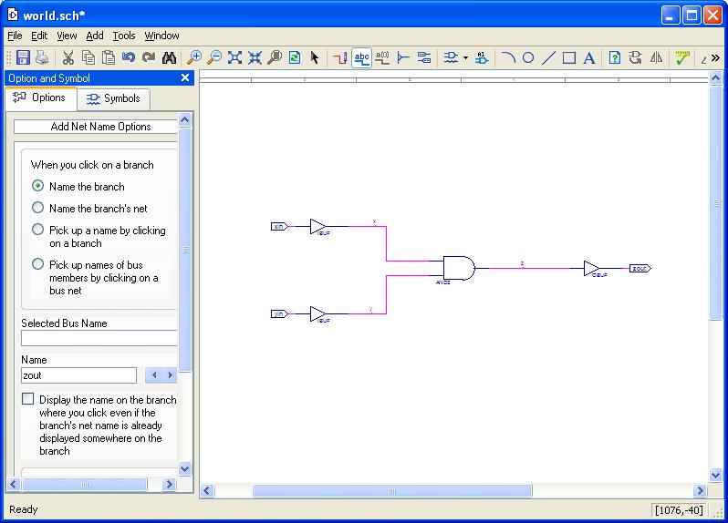
5. Select the IO category and add two ibuf symbols and one obuf symbol as shown below. By convention symbol inputs are on the left and outputs are on the right. (Of course, this no longer holds if you rotate the symbols :)
When a signal is coming into the FPGA an ibuf symbol is used. An obuf is used to indicate a signal that will be an output of the FPGA. Later, by adding attributes to these symbols, you will specify precisely which external pins of the FPGA should be used for these signals.
6. Use the ![]() icon to zoom in on your schematic.
Click on the wire drawing icon
icon to zoom in on your schematic.
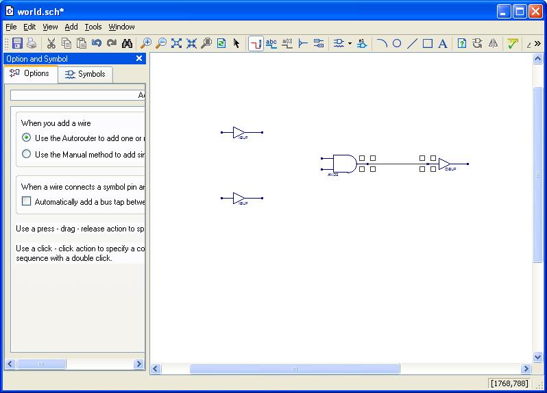
Click on the wire drawing icon ![]() on the toolbar. Position your cursor on the output of the and gate. Click and then move the cursor to the input of the obuf and click again. This should draw a wire between them. When your cursor is positioned on a symbol pin it will change to 4 small squares.
on the toolbar. Position your cursor on the output of the and gate. Click and then move the cursor to the input of the obuf and click again. This should draw a wire between them. When your cursor is positioned on a symbol pin it will change to 4 small squares.
Note the options for adding wires in the left pane. Generally you will want to use the Autorouter.
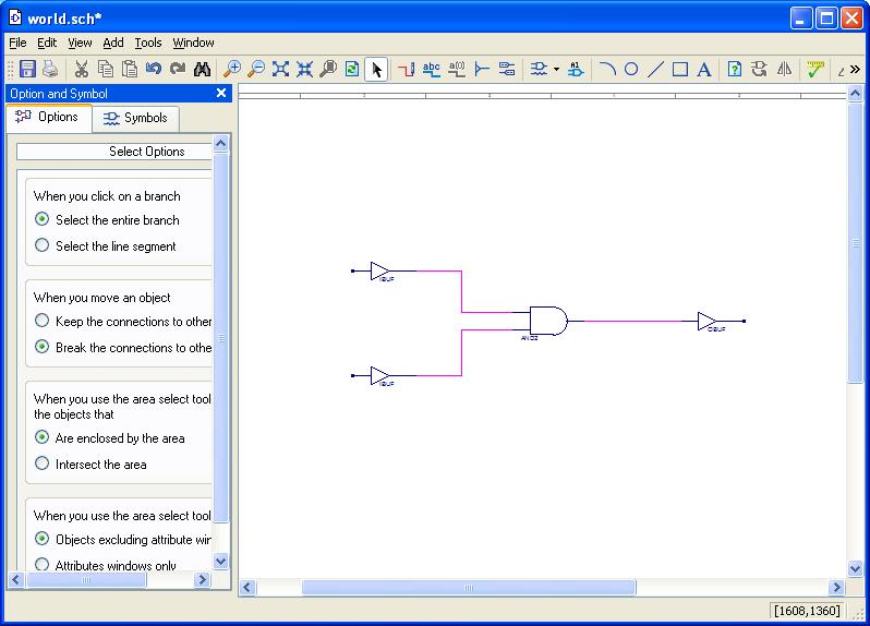
7. Draw two more wires from the ibuf outputs to the and gate inputs.
Note that the wires above are magenta while your wires are dark blue, the same color as the symbols' pins. This makes it hard to tell where the pins ends and the wire starts. (Ask if you would like to know how to change the colors.)
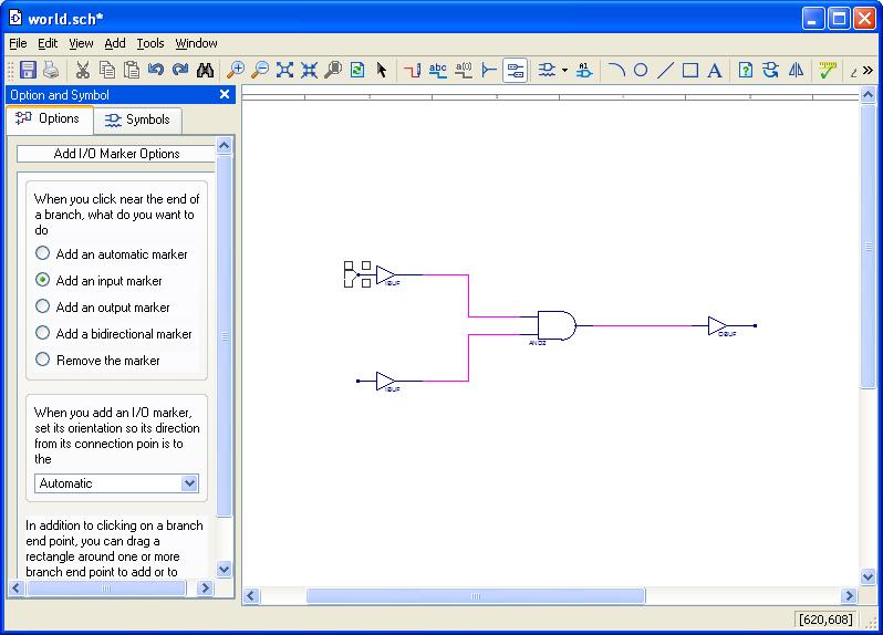
8. Click on the IO markers icon ![]() on the toolbar. Select Add an input marker from the Options pane and move the cursor toe the input of the ibuf symbol and click.
on the toolbar. Select Add an input marker from the Options pane and move the cursor toe the input of the ibuf symbol and click.
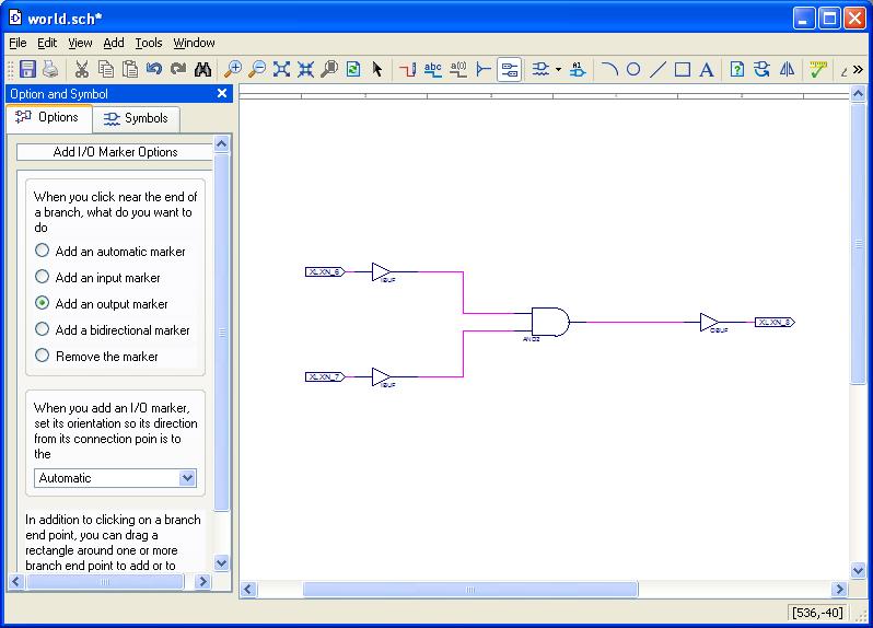
9. Add another input marker to the input of the other ibuf and an output marker to the output of the obuf. (Remember to change the I/O Marker Option in the Options pane for the output marker).
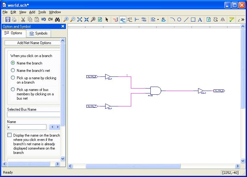
10. To label the wires and markers, click on the label icon ![]() from the toolbar. Type in the label in the Options pane (in this case "x") and click on the wire or marker to label it.
from the toolbar. Type in the label in the Options pane (in this case "x") and click on the wire or marker to label it.
11. Assign labels (names) to all of the other wires and markers; to label a marker click on the wire connected to it. Note that two wires with the same name within a drawing are assumed to be connected even if there is no wire connecting them in the schematic. This is a very useful feature which makes it easy to connect pins without having to draw tangled messes. But it also means you need to be careful not to repeat names for separate signals.
It's important to label wires!!! If you don't label a wire it is assigned a default name, XLXN_#, where # is the next unused integer. It's very difficult to make sense of the simulator output or error reports when your wires are named this way.
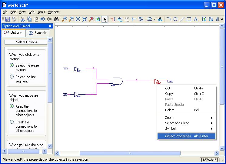
12. To assign a specific pad locations (external pins) on the FPGA, you need to add an attribute to the ibuf or obuf (not the I/O marker!!). Select the obuf (it will turn red) and right click on it. Select Object Properties from the menu.
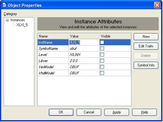
13. The window (below) with the objects attributes will appear. Select New
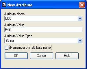
In the New Attribute window (below) select LOC as the Attribute Name from the pull down menu and type in P46 as the Attribute Value. Then click OK twice.
14. The attribute should now appear on the drawing next to the obuf.
You will need to add LOC attributes to all of your ibufs and obufs. Otherwise the tools will use whatever pads they want and it is highly unlikely that they will choose the ones you want.
15. Save your schematic.
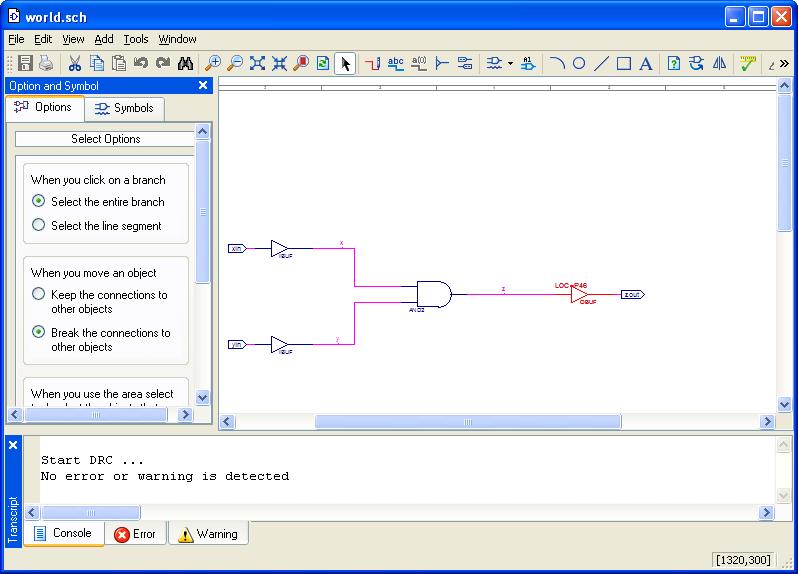
16. Before leaving the schematic editor, it's a good idea to run the Schematic Checker to locate problems at this early stage rather than later. Select Check Schematic from the Tools menu. You should see the following report in the bottom pane:
If not you still have work to do. Select Query from the Tools menu and then click on objects (wires, symbols,etc.) in your schematic to learn about them, if the error is not obvious.
