Difference between revisions of "INV Schematic Tutorial"
(→Creating a schematic view) |
(→Creating a schematic view) |
||
| Line 1: | Line 1: | ||
== Creating a schematic view == | == Creating a schematic view == | ||
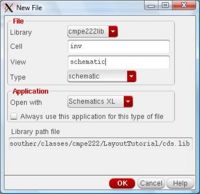
| − | First create a schematic cell view in your library. In the Application Open with | + | First create a schematic cell view in your library manager window by using File->New->Cell View. In the options for "Application Open with" select "Schematic XL". |
[[Image:1-create_cell.jpg|center|200px]] | [[Image:1-create_cell.jpg|center|200px]] | ||
Revision as of 19:17, 23 September 2009
Contents
[hide]Creating a schematic view
First create a schematic cell view in your library manager window by using File->New->Cell View. In the options for "Application Open with" select "Schematic XL".
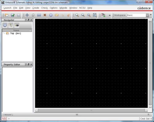
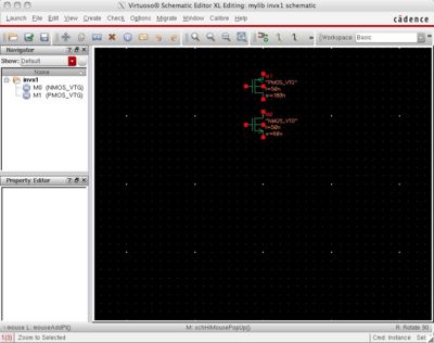
Schematic editor window
When you open a schematic view, it is opened in the schematic editor which looks like this:
A schematic view basically consists of instances, wires, and pins. You can also make buses, but that is not covered in the tutorial.
Creating an instance
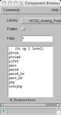
Most of our instances will be of already defined library components. To add an instance, select Create->Instance... or press "i". This will open the Component Browser shown here:
In the component browser, we will only use a few items in the NCSU Analog Parts library. You can use: nmos4 and pmos4 in the N_Transistors and P_Transistors categories; and vdd and gnd in the Supply Nets category. DO NOT USE ANYTHING ELSE. If you use another supply net, it will not work. If you use another transistor, it may not work.
Adding instances
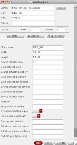
After selecting the comopnent, an Add Instance window will appear like this:
Make sure that you set the appropriate size of the transistor so that it can be matched to your layout. Once you have selected, for example, a pmos device. You can go back to the schematic editor and a pmos transistor instance will be moving around with your mouse cursor. Click on a location and it will instantiate the transistor. If you want to change the instance, use the options in the Edit menu. For supply pins, there are no options you need to set. Add the remainder of the components (vdd, gnd, pmos4, nmos4) for your inverter.
Creating pins
Once you have added the components, you need to add pins for the inputs and outputs with Create->Pins (or press "p"). The pins are used to connect between levels of hierarchy and also to match in the layout. You should use the same names in the schematic and the layout. Name inputs A, B, etc. and outputs Y or Z. Be consistent.
Adding wires
Once you have instantiated the input and output pin, you need to hook everything up with wires. To add wires select Create->Wire (narrow) or press "w" in the schematic editor. You can now point and click everywhere a wire is supposed to go. When you near a terminal you will notice a yellow diamond that shows up. You can press the "s" key to snap the wire to that terminal. This is useful for quickly adding wires and making sure that they are connected to the terminal. If you point and click, it is easy to not really connect the wire.
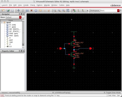
Your final schematic should look like this:
Checking the schematic for errors
You must check the schematic for simple errors before you can save it. Do this by selecting File->Check and Save (or press f8). It will highlight any unconnected pins, for example, before it actually saves the schematic.
Creating a symbol view
If you wish to instantiate your newly created schematic in another schematic, you will first have to create a symbol view. This can be done by selecting Create->Cellview->From Cellview... Press "OK" with the defaults. By default, all symbols are simple boxes.
To change the shape of the symbol, select the auto generated square box and delete it. Draw a new one by select menu Add->Shape->(Choose any shape you want) in the symbol editor.
Design->Check and Save the symbol view just like the schematic view.
Now you are ready to move on to the layout tutorial.
