Simulating a design with ISE Simulator
Simulation allows you to catch many design errors that would be difficult to diagnose otherwise. The Project Navigator translates your schematic into Verilog, and the Verilog code is simulated by the ISE Simulator. Verilog is a language which was developed for architecture simulations back in the 1980's and has evolved into one of the two leading Hardware Description Languages (the other being VHDL). Verilog allows circuits to be described in terms of either their structure (how they are assembled) or their behavior (what they are supposed to do). This makes Verilog convenient for simulation since you can specify the behavior of the environment for your circuit, as well as describe your circuit, and then hook them together and simulate the whole thing.
The steps below use the project and schematics that were previously constructed in the tutorial on Creating a schematic symbol.
Creating a Testbench
Most circuits (but not all) require stimuli (input waveforms) in order to operate. The first step in our simulation is to create a testbench which provides these waveforms, that is, the values for the inputs to your circuit (Unit Under Test).
1. Start up the Project Navigator and open the project you made to create a symbol (or any project with symbols) in the Project Navigator.
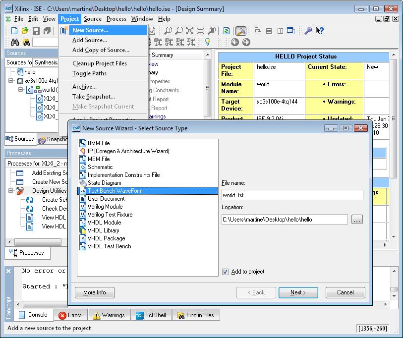
2. In the Project Navigator under the Project menu select New Source ...
3. Select Test Bench Waveform as the type and enter a name. It's a good idea to pick a name that tells you which schematic this testbench is associated with. In the future, you may have different testbenches for different parts of your design. By default this file will be placed in the project directory. Click Next.
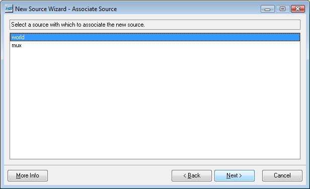
4. On the next screen check that the testbench is associated with the correct source and then click Next.
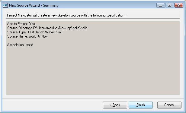
5. Check the information in New Source Wizard - Summary (below) and then click Finish.
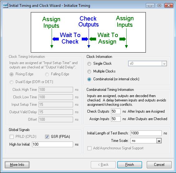
6. The next window will ask you to set and confirm Timing Parameters for your testbench. Since this design is combinational (no clock), the clock parameters are not relevant: select Combinatorial (or Internal Clock) in the top right pane. In the lower right make sure the time scale is in nanoseconds. The length of the testbench is set at 1000ns. It can be extended later. Click OK.
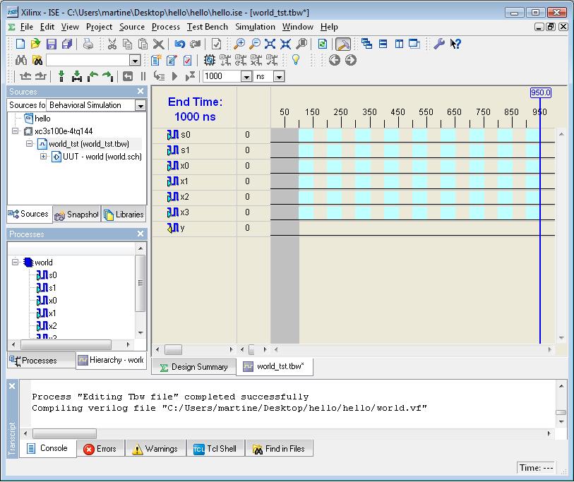
7. The testbench wave tool will appear in the right pane of the Project Navigator. On the left the inputs (blue) and outputs (yellow) are listed. These are the nets in your schematic that had I/O markers. (Do not put I/O markers in your top level schematic just to get the signals to appear here!!!)
8. Pull the wave tool out of the Project Navigator to make it bigger. Click on the waveforms to toggle their values. Be sure to save the file when you are done. If you want to make the testbench longer select Set End of Testbench... from the Test Bench menu.
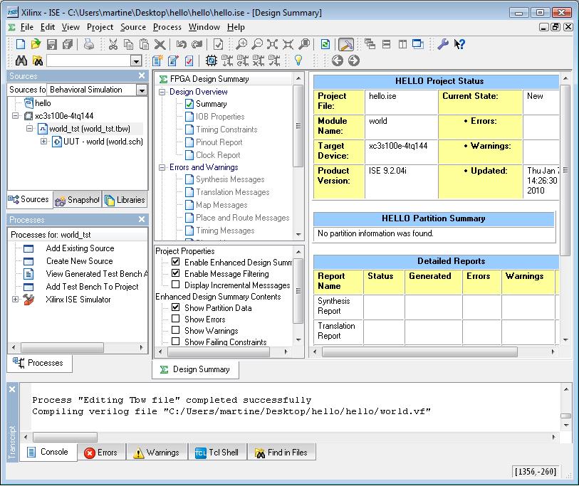
9. After saving your testbench, go back to the Project Navigator. At the top of Sources pane there is a pull-down menu. Select Behavioral Simulation from this menu as shown below.
In the Sources pane you should see your testbench along with the schematic files associated with it.
Simulating your Design
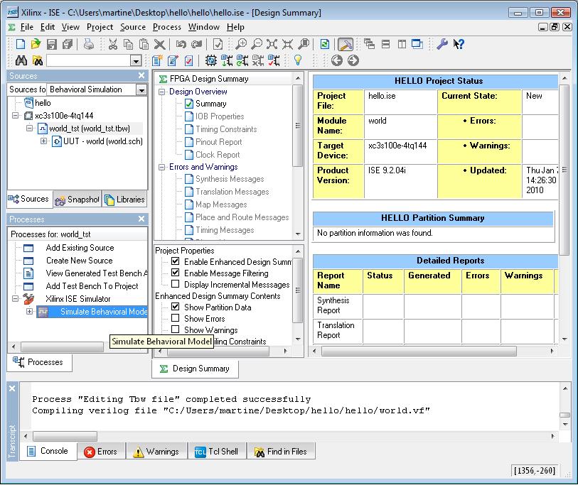
1. In the Sources pane of the Project Navigator select your test bench. The Process window should contain Xilinx ISE Simulator. (If not check the properties of the project to make sure ISE is the simulator: to do this, with the part selected, select Properties under the Source menu.)
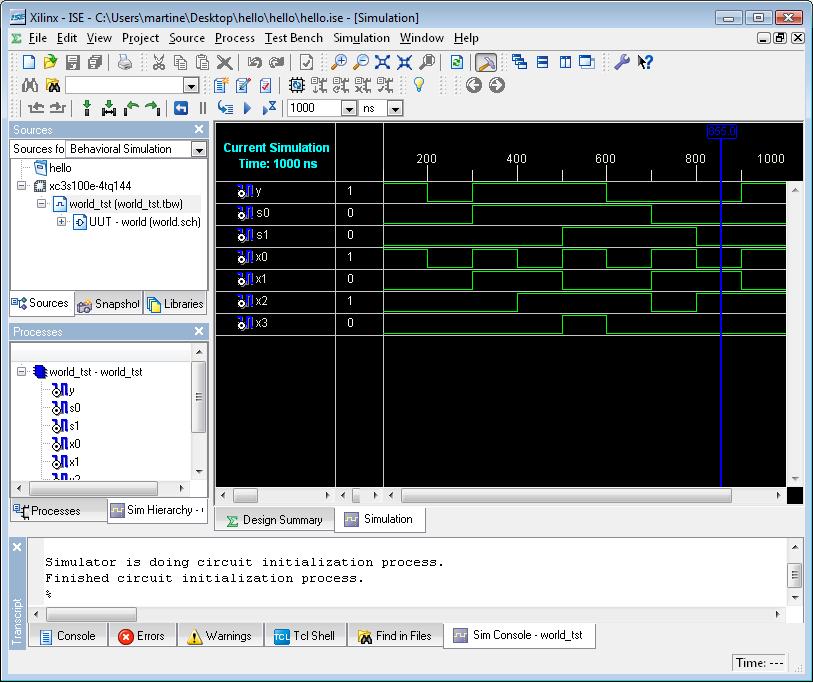
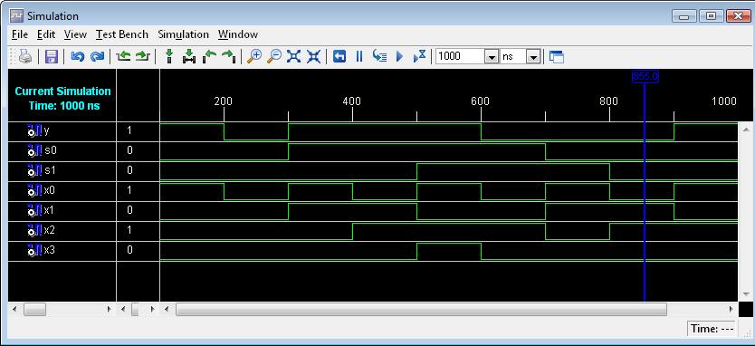
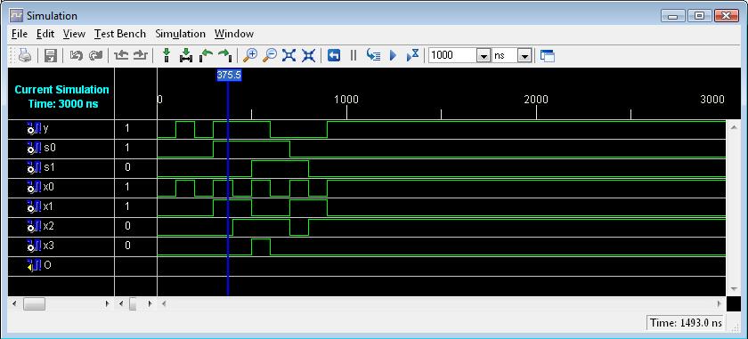
2. Expand the process Xilinx ISE Simulator and double click on Simulate Behavioral Model to start the ISE Simulator. The simulation results should appear in the main pane (after awhile) as waveforms. See below.
3. Pull the waveform window out of the main pane by clicking on the ![]() icon.
icon.
4. You can use the zoom controls ![]() to zoom in and out, or select which section of the simulation to view.
to zoom in and out, or select which section of the simulation to view.
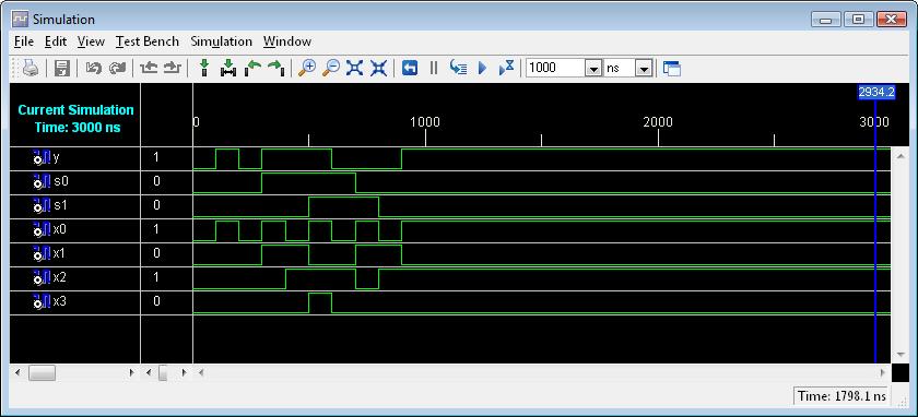
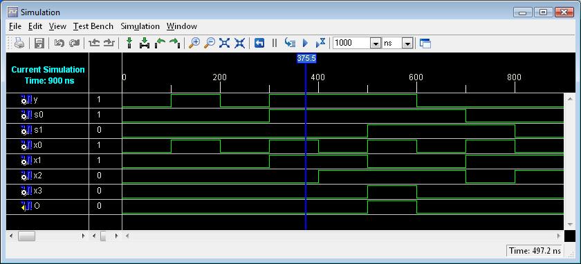
5. You can use the controls just to the right ![]() to control the simulation. The first is "Restart Simlution;" it resets the simulation to time 0 and returns all signals to their initial value. The double bars will stop the simulation if it is running. The "Step" control allows you to step through the Verilog code. The "Run All" control will run your simulation till the end of the testbench. The "Run for Specified Time" will continue the simulation for the amount of time shown in the window. After pressing this last control 3 times and clicking on the Zoom to Full
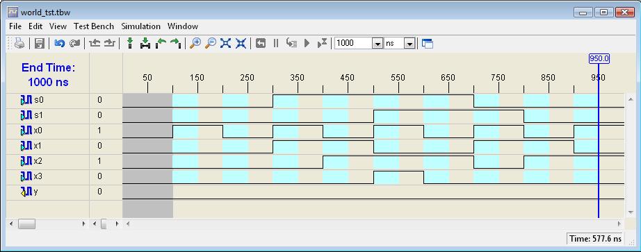
to control the simulation. The first is "Restart Simlution;" it resets the simulation to time 0 and returns all signals to their initial value. The double bars will stop the simulation if it is running. The "Step" control allows you to step through the Verilog code. The "Run All" control will run your simulation till the end of the testbench. The "Run for Specified Time" will continue the simulation for the amount of time shown in the window. After pressing this last control 3 times and clicking on the Zoom to Full ![]() control the Waveforms would look like:
control the Waveforms would look like:
6. The signals listed in the Waveform Viewer are those of the test bench. If you click on the waveform somewhere a blue marker will appear at that time. The values of the signals at that time will appear just to the right of the signal names.
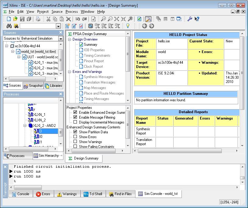
7. You will generally need to see signals other than the top level inputs/outputs in order to determine if your design is correct, and if not, determine the problem. To see other signals, in the Project Navigator, select the tab labeled Sim Hierarchy - world_tst (when world_tst would be your testbench). The top level should be your testbench. If you expand it you will see the signals in your testbench and UUT (Unit Under Test) which is your design. Expand UUT and you will see the symbols and signals that are in your top level schematic. Suppose we wish to see the signal in the first mux coming out of the AND gate. By expanding the first mux (instance XLXI_1) and then expanding the AND inside it we can find the inputs and output of this gate as shown below. (Note that the unnamed intermediate wires have the enlightening net names XLXN_1 and XLXN_2. Tsk, tsk, tsk.)
8. Select the output pin of the AND gate and drag it to the list of signals in the waveform window. This will add the signal to the waveform window but there will be no waveform for it.
9. To see the waveforms of the new signals you must rerun the simulation. Click on Restart ![]() and then click on Run-All
and then click on Run-All ![]() .
.
10. If you want to run the simulation in increments, set the Run Length in the main window to the timestep desired and the click Run for Specified Time ![]() rather than Run-All
rather than Run-All ![]() .
.
The CMPE100 Web: Copyright 2011; Department of Computer Engineering, University of California, Santa Cruz.
