Using Verilog to describe combinational logic
Verilog is a language that was developed for computer architecture simulations back in the 1980's and has since evolved into one of the two leading Hardware Description Languages (the other being VHDL). Verilog allows circuits to be described in terms of either their structure (how they are built) or their behavior (what they do). This is very useful since you can describe how the environment of your design behaves conveniently, without building it, and simulate it along with your circuit. You can also describe the behavior of some parts of your design so that you can simulate the whole design before you finish describing everything. But it's important to keep in mind that anything that is described "behaviorally" rather than "structurally" must be synthesized and the synthesizer is not nearly as capable as you when it comes to constructing efficient circuits. (In fact, the synthesizer wouldn't pass CE100!) That's why when you use Verilog to describe your circuit it is very important to understand how your Verilog code will be translated (synthesized) into logic.
You should begin by reading Section 2.10 of the text which is a short introduction to Verilog. Three versions of a structural description of a 2-to-1 multiplexer written in Verilog are given below.
Please read all the way through because the third (last) version is the simplest fastest method and you will want to use it!
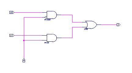
Below is the schematic for a simple multiplexor.
The Verilog code automatically generated for it by ISE is below.
   module mux(s, x0, x1, y);
       input s;
       input x0;
       input x1;
       output y;
       wire XLXN_6;
       wire XLXN_7;
       AND2B1 XLXI_1 (.I0(s), .I1(x0),  .O(XLXN_6));
       OR2 XLXI_3 (.I0(XLXN_7), .I1(XLXN_6), .O(y));
       AND2 XLXI_4 (.I0(s), .I1(x1), .O(XLXN_7));
    endmodule
This Verilog code is a structural description of the same circuit using the symbols from the Xilinx schematic library. (My opinion is that it's easier to draw a schematic than write this code.)
The Verilog code starts with the module declaration which specifies the name of the module followed by its list of the input and output ports. (Inputs first.)
Next the types of the ports are declared along with any "wires" internal to the module.
Following that are the instantiations of the gates(symbols) that comprise the module's structure: in this case 2 AND gates and 1 OR gate. The identifier following the gate/symbol name is the instance identifier. The ports of the gate are associated with one of the wires or ports of the module.
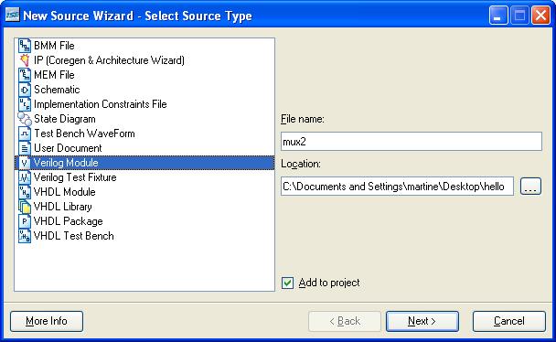
To write Verilog code for a symbol without drawing its schematic, select New Source from the Project menu in the Project Navigator. The following window will appear.
Enter the name of your module, make sure it's being placed in your project directory and select Verilog Module as the source type. Then click Next.
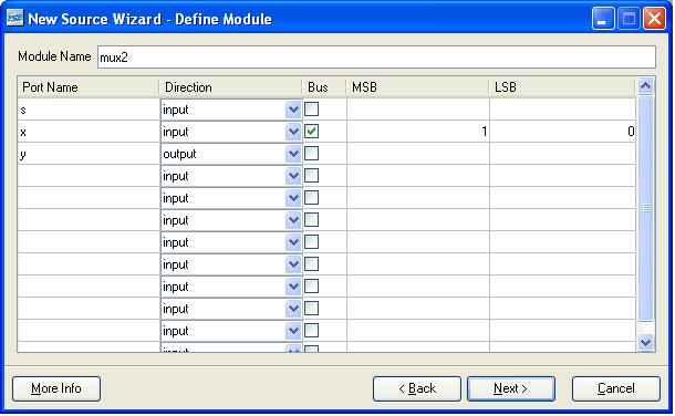
In the window above enter the input and output ports of your module. For a bus check the box in the Bus columns and fill in the MSB and LSB on the right. Otherwise the port is assumed to be a single wire. To change the type of port (input or output) click on the pulldown menu in the Direction column. Click Next when your're done.
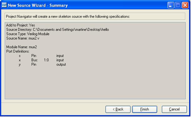
The next window (above) asks you to confirm the information you've just entered. Click Finish if everything is fine, otherwise go back and change it.
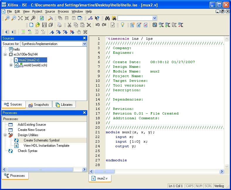
The main window of the Project Navigator will now contain the declaration of your module (see above). The source mux2.v has been added to you project. You can type in the verilog code for your module and then save it.
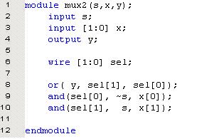
Below a structural description has been entered using Verilog primitives (and(), or()). The outputs of the two AND gates are declared as wires. In this version of the input x was declared as a bus. To refer to bus members use square brackets. (Keep in mind that in schematics parenthesis are used rather than square brackets.)
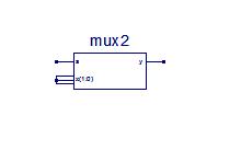
You can create a symbol for your Verilog module in the same way you would if it were a schematic. Select your Verilog module in the Sources window and click on Create Schematic Symbol in the Process window (under Design Utilities). You can then use this symbol in a schematic.
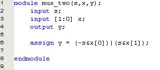
Below is a structural description using an assign statement. This statement associates a logic equation with an output. This uses logic expressions which will be converted directly into the equivalent combinational logic. Note the "|" used as the logical-OR and "&" used as the logical-AND. Do not use "+" or "*"; they have other meanings.
This is the simplest and most specific way to describe your combinational logic.
There are other constructs you can use in Verilog, but these are behavioral and it is quite easy to inadvertently write a behavior that is not combinational. These descriptions use procedural statements that the simulator executes; they will not always produce combinational circuits (even if you think they should).
The CMPE100 Web: Copyright 2011; Department of Computer Engineering, University of California, Santa Cruz.
