FO4 INV Example
From Vlsiwiki
- This assumes that you have a cell (inv in this tutorial) that has a schematic and layout. It is also DRC clean and passes LVS.
- In your schematic view, create a symbol of your design under test (inverter in this case). Design->Create Cellview->From Cellview. The defaults should be correct, but you want to convert from schematic to a symbol view. The Tool/Data Type should be Composer-Symbol.
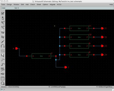
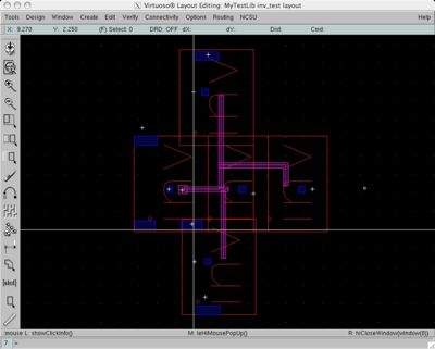
- Create a "inv_test" schematic and layout. In the schematic, you can place your inverter component with Add->Instance and selecting your library and inverter in the component browser. In the layout, you can place an instance of your own cell by doing a Create->Instance... and putting your library name and your cell name in the correct fields. It will then look something like this:

- This is simply an inverter with an fanout of 4 identical inverters. If you add the metal and vias to connect the inverters on metal2, the inv_test layout looks like this when viewing only the top level (via Display->Options). I also added input, output, and vdd/gnd ports at this level too. Make sure the FO4 schematic and layout pass DRC and LVS.

- Refer to Simulation Tutorial on how to simulate the above circuit.