Advanced Testbenches
Contents
Introduction
This tutorial is intended to familiarize you with one possible methodology to test your digital logic. Rather than running UltraSim and visually inspecting the results, you can run a logical (1's and 0's) simulation through the Virtuoso interface. In the previous homeworks, we made schematics using the nmos and pmos devices in the NCSU_Analog_Part library. In addition to the schematic views, these transistors have many other views including a "functional" view. The functional view allows Verilog code of your circuit to be generated from your schematic and simulated. We will simulate your schematic with NCVerilog and view the output in SimVision. Unfortunately, there is no GUI to add stimulus, so you will need to learn a small amount of verilog to design your test benches.
Setting up Logic Simulations
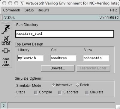
The first step is to open your schematic in Cadence Composer. Remove all of the analog elements from the previous assignments (vpulse, vpwl, vdc, etc.). You can leave the power and ground connected to the transistors in your cells, but do not have any of the "test setup" items. From the menu, select Tools->Verilog_Integration>NCVerilog. You will get a window like this:
If you want to change the time units from ns to ps, select Setup->Netlist. In this view, you can change the global sim time units from ns, the default, to ps. If you change the time units, I recommend that you do this for the global sim precision also. Select OK.
Now click on the "running man" to initialize the design and then on the "hierarchy" button to generate the Verilog netlist from your schematic. You will have to re-do this each time you change your schematic. All of your verilog and run-files are put in the directory specified.
Now, you can select Commands->Edit Test Fixture. In this you can see the test stimulus file is called "testfixture.verilog" by default. You can continue editing this (it will open the file in vi if you press OK) or you can cancel and copy the testbench you previously wrote to this file in the previous run directory (i.e. YourLibrary/nandtree_run1/testfixture.verilog). Keep backups of your testbench in case this gets over-written! It seems that when you click on the running man, it will over-write this file.
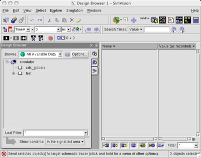
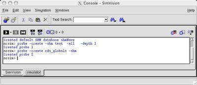
After your stimulus is set up, click the "Simulate" button below the hiearchy button. This will open your verilog and testbench in SimVision. You will get two windows like this:
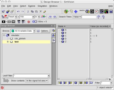
If you select your module in the design browser click on the "Play" button in either window, it will run your simulation in its entirety. On the right side of the design browser, you will see the signals and their final values like this:
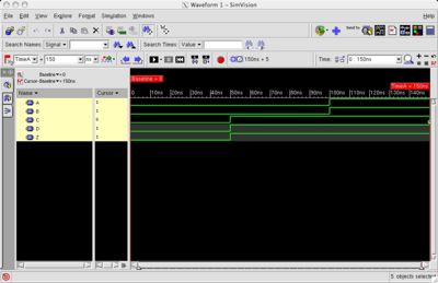
Select the signals on the right that you wish to view and click on the "Send objects to target waveform window" button in the upper right. It is actually the 5th button from the right. This will open the waveform viewer so you can browse your results like this:
Dumping a VCD File for UltraSim
In class, I briefly mentioned that UltraSim can read a Verilog "dump" file. You can generate this file from your verilog simulation. Select the signals you wish to export (i.e. all top level signals). Now select File->Export. Select VCD instead of SST as the format. Change the filename to something meaningful like "mytest.vcd".
You can also dump them from a verilog simulator as shown in the Simulating Verilog tutorial.
Specifying Signal Formats
First, you need to create a .info file to specify the inputs and outputs, the rise/fall times, and the voltage levels. It is a format like this:
.in A B C D
.out Z
.trise 20
.tfall 20
.vih 1.8
.vil 0.0
.voh 1.3
.vol 0.5
You can call it something like "mytest.info". The voltage levels are in volts. The trist and tfall times are in the same units as your Verilog simulation (ns or ps).
Reading Digital Inputs in Ultrasim
You can include the VCD and info file in your spice file like this:
*ultrasim: .vcd
*ultrasim: + "/mada/users/user/CMPE223/verilog/simulation/test.vcd"
*ultrasim: + "/mada/users/user/CMPE223/verilog/simulation/test.info"
In the UltraSim GUI, you can do the normal setup, but don't add the test structures to your schematic. Instead, select Setup->Simulation Files and put the path and name of the VCD file and .info file in the appropriate fields.
Viewing Digital Outputs
But there's a better way to view waveforms- after some digging, here's what I ended up with:
- Run the simulation while changing simulation->option->analog->OutputFormat->SST2
- Use simvision to Open the resulting database (which is probably in <HOMEDIR>/Cadence/...
- You get really nice waveforms, and the ability to group signals into buses which is for the adders etc.
Here's a nice screenshot got from simvision, so you can see what it can do
Busses
Busses are allowed in both Composer and Verilog. In composer, you can make a bus "pin" by just naming it, for example, "A<0:3>" for an 4-bit bus. You can add a bus pin in Composer by adding a pin like normal but using the bus name, "A<0:3>". Now, suppose you want to use only the "A<0>" bit for the input of a gate. Connect a wire from the pin as normal. Select the unique part of the wire (right by the single-bit pin, not the bus pin) and select Add->Wire Name from the menus. Input the individual bit name like "A<0". Now, you place the name with one click and then you draw a line to the wire that the name corresponds to with the second click.
In your layout, you must make a pin for each bit, A<0>, A<1>, etc.
In Verilog, the names use square instead of angled brackets, "A[0:3]". The most common problem with busses is assigning them in the wrong order. "A[0:3]" and "A[3:0]" are not the same. Be consistent and it won't be a problem. To the previous VCD information file, you need to append any correspondence information about bus names. For example, the inputs become
.in A[0:3]
And we must convert the bus naming style to one that the schematic is using with this command
.alias *[*] *_*
In your verilog stimulus file, you can specify busses in a number of ways. For example,
eightbitbus[0:7] = 8'h0F;
eightbitbus[0:7] = 8'b00001111;
The first assigns 8 bits as hexidecimal. The second does it with binary.
Automatic result checking
To Automatically check result with verilog dump (VCD) file in Ultrasim, add this line in to your .info file.
syntax:
.chkwindow <start_time> <end_time> <steady> [period=integer] [first=integer] [signal_name1... signal_nameN ]
example:
.chkwindow 0 5 0 period=40 first=30 out[*]
It tells ultrasim to activate periodic window of size 5 (end_time-start_time) checking for signals out[*] (signal_name). The check points start at 30 ns (first=30) and repeats every 40 ns (period=40).
Then you will get a file called input.veclog in your simulationg directory cse/grads/<username>/cadence/simulation/<test_module>/UltraSim/schematic/psf/input.veclog
This file is like this:
****VectorCheck for out_0: All good!
Number of total vector checks = 8
Number of X's matched correctly = 0
Number of Zero's matched correctly = 6
Number of One's matched correctly = 2
Number of total states matched correctly = 8
Number of total errors = 0
You can find how many zero or one are mached correctly.
Summary
After this tutorial, you should be able to quickly write test benches in Verilog, run them in NCVerilog and import the results into UltraSim. This will greatly improve your ability to test your circuits.
