Lithography Simulation
In this tutorial you will create a layout, analyze it using Calibre's Litho-Friendly Design package, and use layout techniques to improve your yield.
Acknowledgements: NCSU EDA Wiki
Create a New Layout
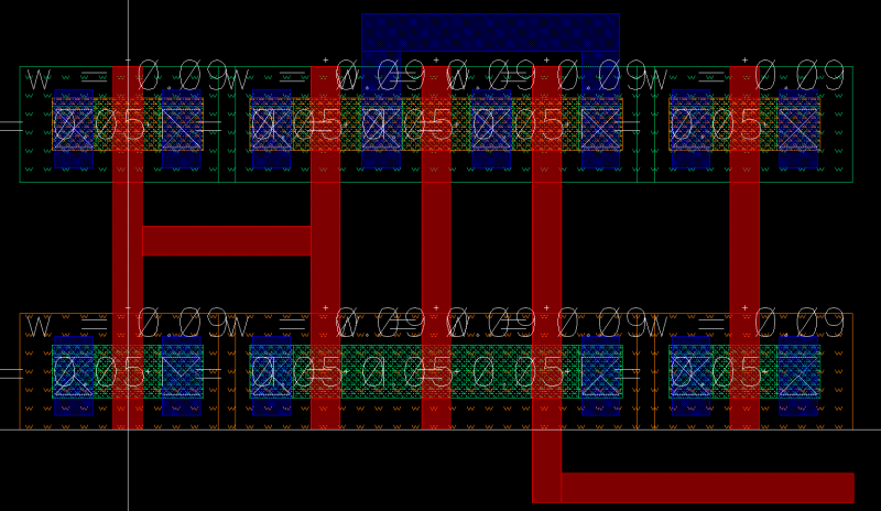
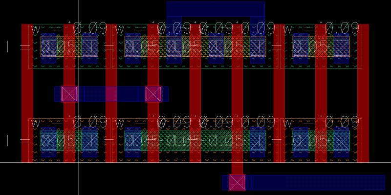
You can create a new layout of say, inverter or use any existing layout from your own library. An example layout is shown below:
Run LFD on Your Layout
You can run LFD by selecting Calibre->Run DRC from the menu bar, which brings up the Calibre Interactive window. Load the LFD runset file by selecting File->Load Runset from this window, and typing in ".runset.calibre.lfd". (Note: If you are prompted about whether or not to save the current runset file, I would click "no".) Then click "Run DRC."
LFD flow shows the printing range of the drawn object. Open the process variability bands results database in the RVE window by clicking File->Open Database... and selecting the file lfd_pvband.rdb.
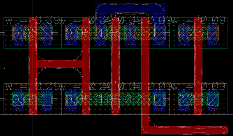
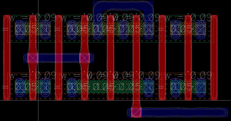
You can highlight the worst case metal pvbands by right-clicking on "Check lfd_pvb_metal1_p3" and selecting "Highlight Cluster." Then you can also highlight the worst case poly pvbands by checking "Check lfd_pvb_poly_p3". Your layout should now look like this:
Note that, in some regions, polysilicon lines have PV bands which are significantly narrower than the drawn width. PV-bands are aware of the layout-induced variations, meaning the bands are different for the same object having different neighboring properties. As can be seen from the pv-bands, the right-most polysilicon line has the narrowest possible width since it does not have any polysilicon neighbor close to it. Printed gate length is very important for circuit performance since it affects the Ion current. More dramatic variation is on drain leakage current (Ioff) since a device threshold voltage (VT) has an exponential dependence on the gate length of the device [1]. This can cause large variation between devices, which is not desirable. In this case, we do not want polysilicon lines to have PV bands narrower than 37.5nm. These regions can be observed from the RVE window by clicking File->Open Database... and selecting the file lfd_error.rdb. Then you can highlight the errors by right-clicking on "Check lfd_poly_MWC_p3" and selecting "Highlight Cluster." These rectangle regions are the ones where poly have a width smaller than 37.5nm. In addition check "lfd_metal1_MWC_p3" where the metal1 width is narrower than 45nm since narrower metal1 lines increases resistance on the interconnect, which slows down the circuit. Your layout should now look like this:
The lfd_error.rdb file will serve as our main evidence that the design has "passed" the LFD rule check and is good for fabrication, even if the layout fails a normal DRC check. The LFD simulation gives us a more accurate idea of the variation that is likely to occur during fabrication, but it's impractical to use this type of simulation for the entire chip, because it would take too much time. Therefore, LFD simulations are normally performed on cells that occur very often in the design and are critical to the overall performance, such as an SRAM bitcell.
Since the lfd_error.rdb file is so important, open it up in a text editor to see what it looks like. You should notice from the Calibre - DRC RVE window that the rule that's failing is called "lfd_metal1_MWC_p3". Scan forward in the file to the line that contains this text, and you should see the following:
lfd_poly_MWC_act_poly_p3
16 16 3
lfd_metal1_MWC_p3
2 2 3
The first line gives the name of the rule, and the "16" & "1" that begins the second line shows how many errors there are that need to be fixed. It's inconvenient to have to check for errors this way, but until we learn better how to write Calibre LFD rules, this is how we need to do it.
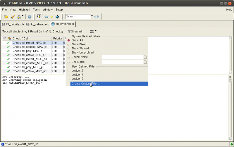
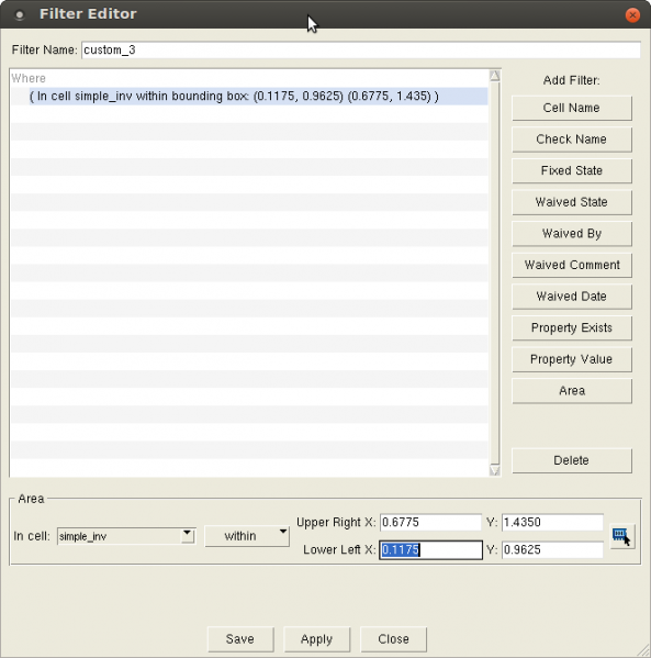
To be able to view errors pertaining to a select area, you need to setup a custom filter as follows: In the Calibre results window, click on the tab marked Show All, and click on Create Custom Filter as depicted in the image below
In the new form, fill the X and Y co-ordinates of interest at the bottom of the form and click Apply
Fixing the LFD Errors
Here are the ways that we can fix these errors:
- In general, what makes lithography at these small dimensions so hard is that we have drawn right angles, but it's easier to print smooth curves. The mask-generation tools are doing their best to give us what we want, but they have limits. DRC rules are minimum design rules that constraints on critical process step requirements such as printability. However DRC rules does not take process variation and variability into account. With the scaling of CMOS technology, restrictive design rules(RDR) are introduced for regular layout which takes care of process variation as well as design for manufacturability (DFM) and design for yielf (DFY) [2]. As can be seen from the errorbands, the layout has minimum poly width errors in the isolated poly lines (on the leftmost and rigthmost) since they do not have poly lines near them. In addition horizontal poly lines create ringing which creates also minimum poly width errors. For the correction,a regular layout, which includes poly lines only in vertical direction and which are periodic, in other words they have poly neighbours at a regular distance. Therefore, dummy poly lines are introduced just to decrease the variation. These two rules prevent poly to become narrower than desired and remove LFD errors.
- There is also a minimum metal1 width error on the metal line which is on top because of the metal 1 contact near it. This can be corrected by increasing to metal1 to metal1 spacing.
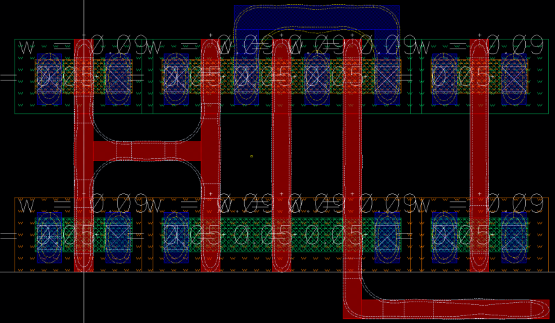
The fixed layout is shown below:
You can open the Corrected_layout from library manager and run LFD on the Corrected_layout and check the lfd_pvband.rdb and lfd_error.rdb file as mentioned above. After the corrections, your layout should be LFD clean which means you should not have any LFD minimum width violation for poly and metal1. Looking in the file, you can scan forward to the previous error and see something like the follwoing:
lfd_poly_MWC_p3
0 0 3
lfd_metal1_MWC_p3
0 0 3
The "0" that begins the last line indicates that there are no errors. Finally you can highlight the pvbands as mentioned previously. Your layout with pvbands becomes as follows:
After the updates we not only solved the problems but also reduced the variations through the poly and metal1 pvbands. If you look at the pvbands of the first and updated layout, you see that the latter one has more straight pvbands, which means it is less susceptible to resistance variations. For the purposes of this course, however, a layout will be considered "correct" if it has no error markers in the lfd_error.rdb file AND if it passes a normal DRC check. Note that the LFD check is considering only the layers active, contact, poly, and metal1, which have the smallest features in this technology.
Congratulations! You are done!
 References
 [1] A. Bourov, et al., “Experimental measurement of Photoresist Modulation curves”,
Proc. SPIE, pp 1003–1008, 2006.
 [2] A.R.Subramaniam, et al. , "Model-Based Prediction and Optimization of Restrictive Design Rules",
Submitted to IEEE Transactions on Circuits and Systems
