Select
Contents
Block Diagram
Design Specifications
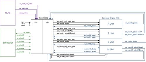
The select stage is between the Scheduler and the Compute Engine (CE). The main purpose of this unit is to avoid RAW hazards between clusters and to enforce structural hazards due to limited amount of units available. The select unit has two stages: SE0 and SE1. Each stage is processed in one clock cycle. There is also an overlapping stage of CE0 between the Select module and CE module. The select module takes in 4 instructions per clock cycle. Each instruction is put into a FIFO queue. There are 4 queues and each hold 8 instructions.
|
|
|
Each of the four clusters in the CE holds 128 registers in its Register File. There are a total of 512 registers. A 9-bit binary number is assigned to each register. Since there are only 640 registers, the highest 3-bits are indicative of the CE cluster/unit to which they belong.
| Register Number | Highest 3 bits | Compute Engine (CE) |
|---|---|---|
| 0 - 127 | 000 | A Unit RF |
| 128 - 255 | 001 | B Unit RF |
| 256 - 383 | 010 | C Unit RF |
| 384 - 511 | 011 | L Unit RF |
| 512 - 639 | 100 | S Unit RF |
There are three vectors called READY, SCHEDULING, and PENDING and each have 640 rows with one column. The value of each element is either 0 or 1. The horizontal index is the register name/position. The READY vector is initialized to all x’s. The SCHEDULING and PENDING vectors are both initialized to zeros.
|
|
|
|
READY bit
It represents the fact that the contents of a register are ready to be used. When a register of an instruction is not ready, the ready bit is set to 0, and when the DONE signal from the CE is received and the content of the destination register becomes valid, it is set to 1. In other words
@ SE0:
      READY [DINST.DEST] = 0
@ WB stage of the CE:
      READY [DINST.DEST] = 1
SCHEDULING bit
At the first stage, SE0, the scheduling bit for the destination register is set to 1 upon reading. When the instruction has been successfully sent out and the corresponding CE resource is not busy, the scheduling bit of the destination register is set to 0.
@ SE0:
        SCHEDULING [DINST.DEST] = 1
@ CE0: //if sent & !busy
        SCHEDULING [DINST.DEST] = 0
PENDING bit
This bit is required to let the CE know when the content of a register from an external source is needed. For example,
RA1 ← RA2 + RB1
The arithmetic operation is taking place in the aunit of the CE. The source register, RB1, is located in the Register File of the bunit. Therefore, there needs to be a signal which lets the BUnit know in advance to forward that particular register to the aunit. The signal is simply the address of the RB1 which is to be forwarded to aunit. Before the forwarding is performed, the PENDING bit is set to 1. As it can be concluded the pending bit is set or reset based on the source registers. Another important point to remember is that the register has to be ready. Meaning, the READY bit has to be set before any forwarding is issued. The more complete check for forwarding is performed as follows:
IF (READY & PENDING)
        SEND it to be forwarded //send the address
A challenge of waiting until (READY & PENDING)[dinst.src1] is true is that it is never possible to send an instruction and the do the forwarding simultaneously even if the register is ready. The reason is that it requires one cycle to set the pending bit.
The solution can be to set the FWD value if the register is READY. Since there can be many instructions and structural hazards for the forwarding port, the select stage (SE1) should decide which instruction gets the value forwarded. If an instruction got a value forwarded the pending bit should be cleared.
The pending bit is cleared when forwarding is finished.
@ CE0:
        //setting to 1
         IF (DINST.SRC1.id	!=  DINST.DEST.id)
            PENDING [DINST.SRC1] = 1
         IF (DINST.SRC2.id	!=  DINST.DEST.id)
            PENDING [DINST.SRC2] = 1
        //setting to zero whenever a forwarding is done
         PENDING [fwd] = 0
We can send up to 4 forwarding signal in each clock cycle.
# AUNIT  - se_aunit_fwd_pos
# BUNIT0 - se_bunit_fwd_pos
# BUNIT1
# CUNIT  - se_cunit_fwd_pos
# LUNIT  - se_lunit_fwd_pos
# SUNIT0 - se_sunit_fwd_pos
# SUNIT1
How to Compile
In order to compile any of Select Modules, go to directory Select and type in
rake fpga:<ModuleName> full=1 v=1
rake asic:<ModuleName> full=1 v=1
This will create a script.
./synplify_ModuleName.sh
Run the shell script to create an srr file in synplify directory which will be named ModuleName.srr Open this file in any editor and look for errors and warnings. If you would like info about the timing just find "MHz". If you would like to specify the line numbers of errors and warnings just type in the following command in the select directory.
grep @E synplify/ModuleName.srr
--Elnaz 22:14, 27 March 2009 (PDT)
