Difference between revisions of "INV Layout Tutorial"
(→Opening the new cell view) |
(→Opening the new cell view) |
||
| Line 8: | Line 8: | ||
After this, press "OK" and then in the Library Manager, select your new library, the cell, and the "layout" cell view that you just created. You can also create a "schematic" view which will be in another tutorial, but is very similar. | After this, press "OK" and then in the Library Manager, select your new library, the cell, and the "layout" cell view that you just created. You can also create a "schematic" view which will be in another tutorial, but is very similar. | ||
| − | [[Image:8-lsw.jpg|center|100px]] | + | [[Image:8-lsw.jpg|center|100px]][[Image:7-layout_editing.jpg|center|300px]] |
| − | + | ||
| − | [[Image:7-layout_editing.jpg|center|300px]] | + | |
Revision as of 03:45, 28 September 2007
Contents
[hide]Creating a layout cell view
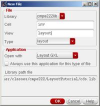
First create a layout cell view in your library. If you have not created a library, see the Technology Setup document.
Opening the new cell view
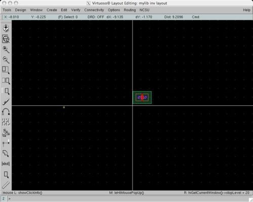
After this, press "OK" and then in the Library Manager, select your new library, the cell, and the "layout" cell view that you just created. You can also create a "schematic" view which will be in another tutorial, but is very similar.
The LSW window has a lot of options. The layer with the black box around it is the current drawing layer. In addition to this, however, you can also make layers invisible and unselectable. The "AV" and "NV" buttons stand for all visible and none visible, respectively. This will work on every layer except the one that is current selected for drawing. Similarly, the "AS" and "NS" buttons stand for all selectible and none selectible.
Creating an instance
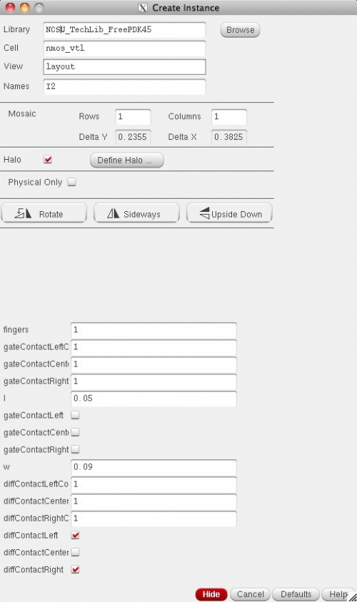
Once you have the layout cell view open, you are free to start adding layout. There are many tools to do this, but a few are the most important and are covered in detail. You should play with the commands and figure out other, more efficient, ways of doing things. To create a transistor, our development kit has "P Cells" set up. These are parameterized transistor cells that automatically draw the gate, diffusion, and source/drain contacts.If you do not want the "standard" transistor, you are free to draw all of these shapes on your own, but it is more work.
Browse library
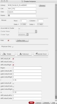
If you click on "Browse" in the create instance window, it will open another window that shows your technology library. There are a lot of goodies in here including vias, transistors, and well contacts (taps). The vias can make an array of arbitrary size and the transistors can be modified for different sizes, folds, etc. We show how to create a PMOS device here.
Placing the instance
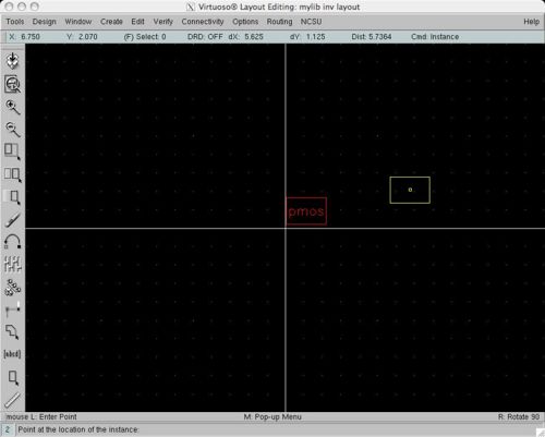
If you go back to the layout window, you now have an instance attached to your mouse cursor that floats wherever you move. If you click, it will instantiate a copy of the instance. It will continue instantiating copies until you press escape.
If you place too many copies, you can select an instance by clicking on it and hitting "d" for delete. Other useful functions that operate on selected instances are "c" for copying and "m" for moving.
Changing the view
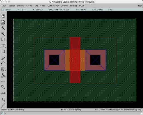
Now the instance is placed but you only see a red box. By default, you don't see inside the instance. To change this, press Shift-f which will view all levels of the hierarchy. You can also select fewer levels in the View menu.
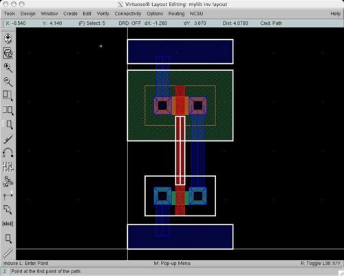
Once you do this, you see something like this:
You can also zoom in and out. To fit the layout in the current window, you just press "f" in the layout window. Zooming out is done with "Z" and if you press "z" you can select an area to zoom to.
Adding paths
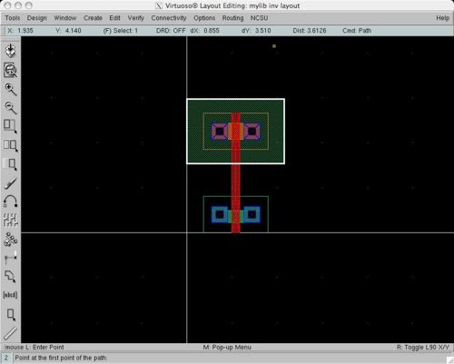
Now we assume you can add an NMOS transistor as well. Once you do this, you will want to connect the poly gate. You can do this by clicking on "poly" (red) in the LSW. Whatever layer is highlighted is what you will create shapes on. In the layout window, you can press "p" to create a path. A path is a polygon of minimum width that is used to speed up routing by hand. In this case, we just want a straight rectangle, but we could also add an arbitrary shape. Again, to delete a path, select it and press "d".
Adding Rectangles
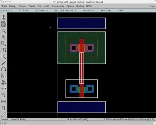
We do not want all shapes to be the minimum width. Supply rails, for example, should be thicker to handle larger amounts of current without dropping the voltage due to resistance. To create a non-minimum width, we must create it with the rectangle (or polygon) tool. To draw a rectangle, press the "r" key and then click and drag. You can copy the rail by selecting it and typing "c" to create the other supply rail. Once it is copied, you can also move them with "m".
Stretch tool
Another tool that is useful is the stretch tool. If you create a rectangle, for example, but it is not quite right, you can first type "s" to get in to the stretch tool mode. Now you can select a SIDE of the rectangle and move it. Connect the remainder of the diffusion areas to power, ground and the output as appropriate in an inverter.
Creating pins
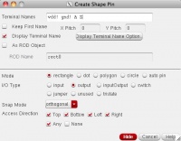
Once you are done connecting the nets, the layout is technically done. However, we need to add pins so that LVS can match the layout to the schematic and so that you can connect to the internals of the cell without having to look inside all the time. This is useful at higher levels of the design hierarchy to speed up the display by reducing the number of visible polygons.
Once you create the pins for the inputs, outputs, and vdd and gnd, you are done with the layout. However, now, you need to run LVS to make sure that it matches the schematic and DRC to make sure that you didn't violate any design rules.
